Summary
The NPU vs GPU difference comes down to design focus. A GPU is a general-purpose parallel processor in which many cores run the same operation in parallel; an NPU is a dedicated accelerator built around multiply-accumulate (MAC) operations for neural networks. This post compares them by structure, training versus inference, and power and use case, for beginners and embedded developers.
One-line answer: A GPU is a flexible general-purpose parallel processor, and an NPU is a neural-network accelerator built around a MAC array. The difference is not “a GPU can’t do matrix math” but design focus: flexibility versus a mostly fixed dataflow with on-chip memory, and power.
What are an NPU and a GPU?
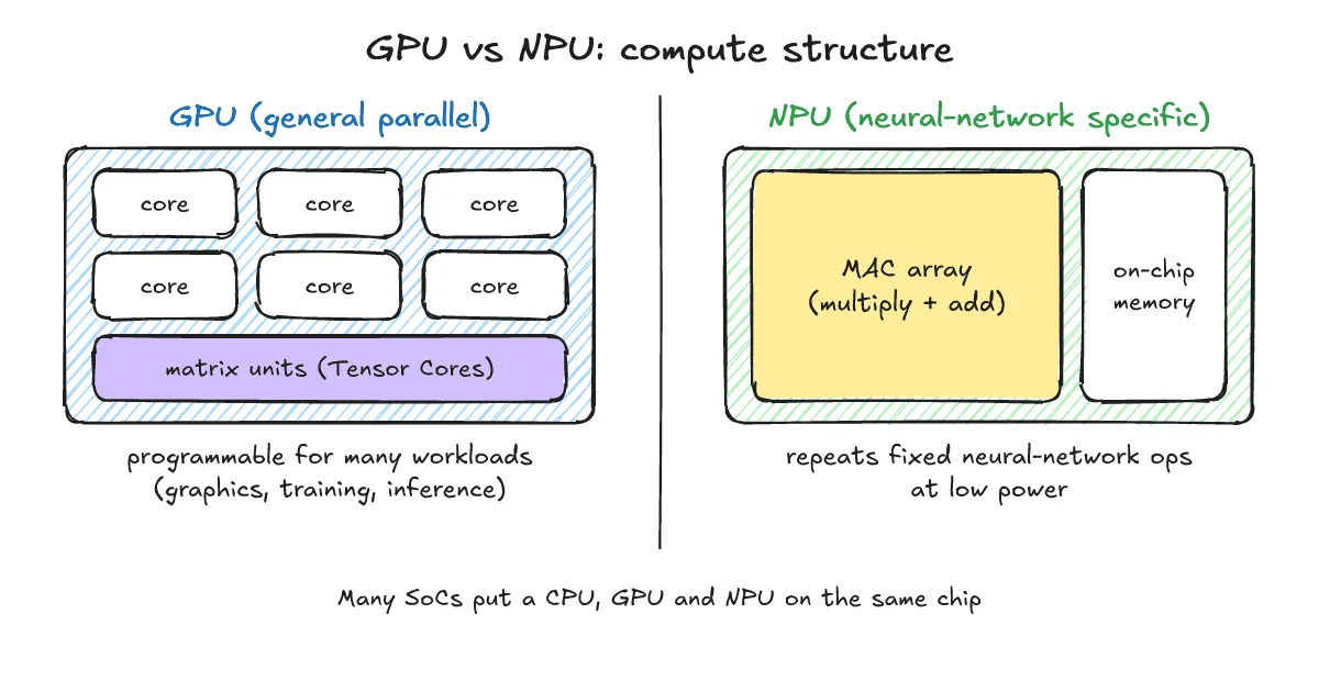
One-line answer: The starting point of the NPU vs GPU difference is that a GPU is a general-purpose parallel processor originally made for graphics, while an NPU is a dedicated accelerator tuned for the multiply-accumulate (MAC) work in matrix multiply and convolution.
A GPU was originally built for graphics. Many cores run the same operation in parallel, and programming models such as CUDA let you run many kinds of work beyond graphics.
An NPU is a dedicated accelerator for neural-network math. Most of a neural network is matrix multiply and convolution, which are repeated MAC operations, and an NPU is designed to run exactly those efficiently.
It is common for a CPU, a GPU and an NPU to sit together in one chip (SoC). So it helps to ask “which job goes where” rather than “which is better”.
How is the structure different, and what are matrix multiply and a MAC array?
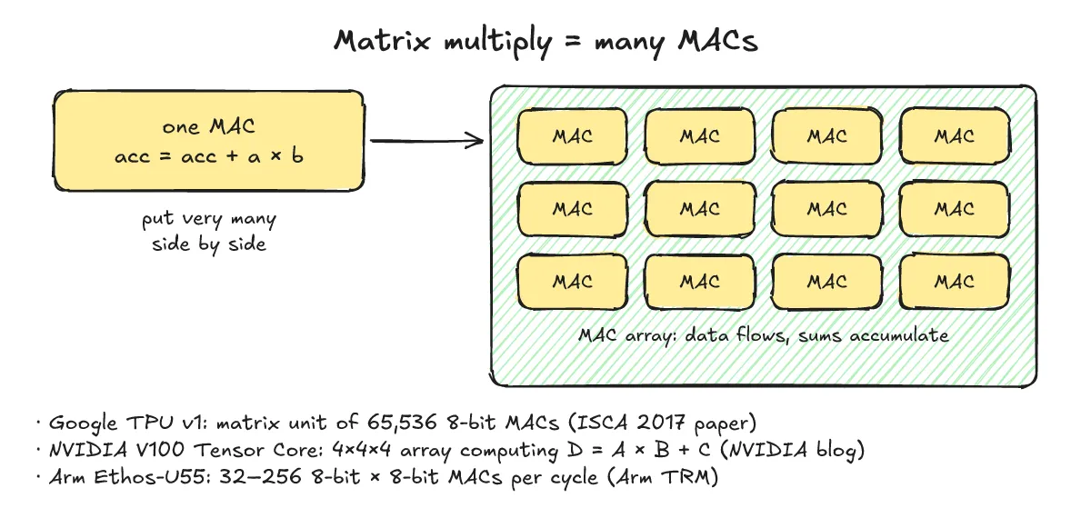
One-line answer: MAC means multiply and accumulate (acc += a×b), and matrix multiply is MAC repeated. An NPU lays out MACs as an array tied to on-chip memory, while GPUs now have matrix units (Tensor Cores) too, so the gap is one of degree and design focus.
MAC (multiply-accumulate) multiplies two values and adds the result to a running total. Matrix multiply is that operation repeated a great many times.
// Concept example (not executed)
acc += a * b;
TPU v1: The TPU v1 paper (Jouppi et al., ISCA 2017) says “the heart of the TPU is a 65,536 8-bit MAC matrix multiply unit”, with a peak of 92 TOPS and 28 MiB of software-managed on-chip memory. It has been deployed in datacenters since 2015 and accelerates the inference phase. The paper also describes a deterministic execution model, in contrast to the time-varying optimizations of CPUs and GPUs (caches, out-of-order execution, multithreading and so on). The TPU itself is covered in the TPU post (Korean).
NVIDIA Tensor Cores: According to the NVIDIA Technical Blog (Programming Tensor Cores in CUDA 9), each V100 Tensor Core is a 4x4x4 matrix processing array that performs D = A * B + C, where A and B are FP16 and C and D are FP16 or FP32. A warp uses them together for a 16x16x16 matrix multiply-accumulate (MMA) through the WMMA API. The Turing Tuning Guide (NVIDIA Turing Tuning Guide) adds that Turing Tensor Cores support integer matrix multiply with 8-bit, 4-bit and 1-bit inputs and 32-bit integer accumulation.
Arm Ethos-U55: According to the Arm technical reference manual (Arm Ethos-U55 NPU TRM 102420), the Ethos-U55 microNPU is configurable from 32 to 256 MACs per clock cycle, each an 8-bit x 8-bit MAC. The MAC unit performs the multiply-accumulate for convolution, vector products and pooling, and the NPU is designed to work with Cortex-M.
In short, GPUs now have matrix units (Tensor Cores) too, so “a GPU can’t do matrix math” is wrong. The difference is design focus: a GPU combines general programmability with matrix units, while an NPU is built around a MAC array and on-chip memory with a mostly fixed dataflow.
How do training and inference split the use?
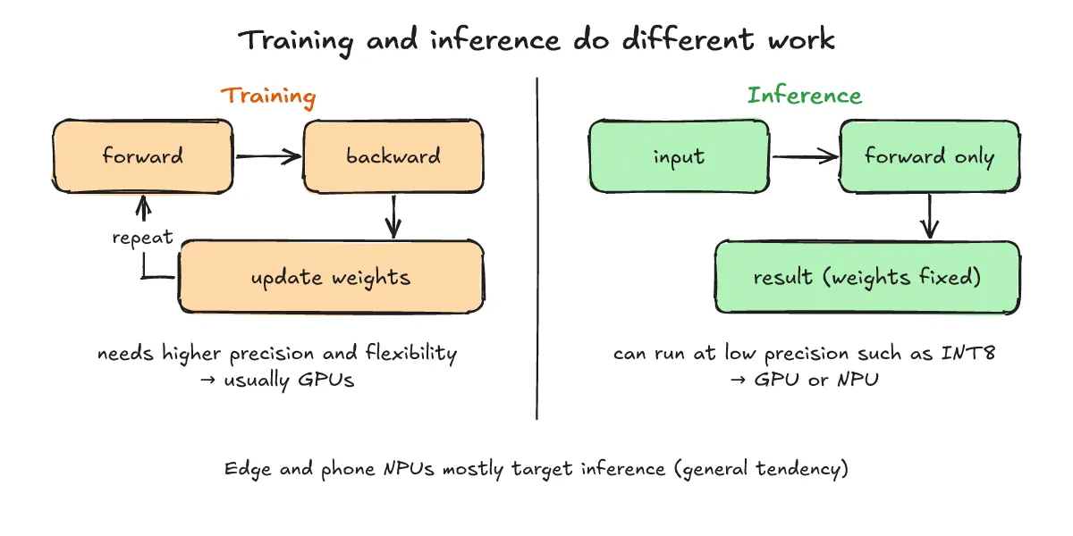
One-line answer: Training (forward pass, backward pass and weight update, repeated many times) needs higher precision and flexibility and is commonly done on GPUs; inference (forward pass only, with fixed weights) is where many NPUs aim.
Training repeats the forward pass, backward pass and weight update many times. It usually relies on floating-point precision such as FP16, BF16 or FP32 and a wider range of operations, so GPUs are the common choice.
Inference runs only the forward pass with fixed weights, so lower precision such as INT8 can be used. That is why many NPUs in phones and edge SoCs target inference. The Ethos-U55 above uses 8-bit MACs (Arm TRM), and the Rockchip RV1126B NPU is listed at “3 TOPS @ INT8” (Forlinx product page); more on that in the next section. TPU v1 itself was an inference accelerator (TPU v1 paper).
Some later datacenter accelerators also handle training. This post does not go into specs; see the TPU post (Korean). Quantization is not explained in depth here, and for LLM inference see the AI study Day 3 post on LLM inference and the KV cache (Korean).
Which should I choose by power and use case?
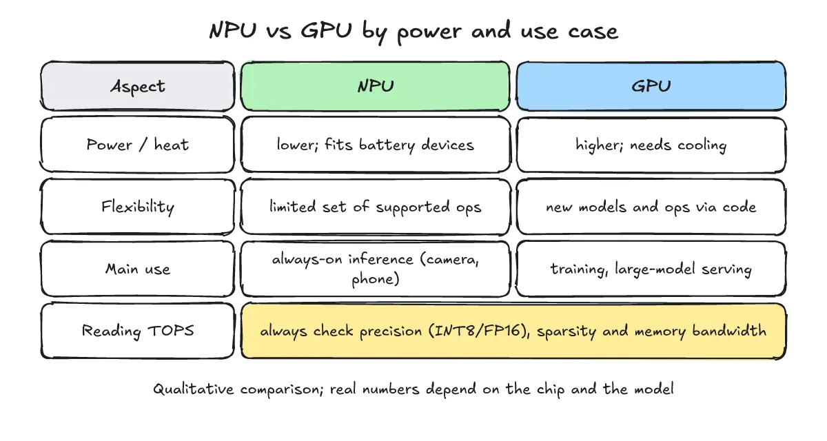
One-line answer: For low-power, always-on, battery or edge devices running fixed models, choose an NPU; for flexibility, training, large models or new operators (with more power and cooling), choose a GPU.
| Aspect | NPU | GPU |
|---|---|---|
| Purpose | Dedicated neural-network acceleration | General-purpose parallel processing (graphics, many workloads) |
| Compute unit | MAC array + on-chip memory | Many cores + matrix units (Tensor Cores) |
| Precision (mainly) | Mostly low precision such as INT8 | Broad support: FP16/BF16/FP32 and more |
| Programming flexibility | Limited operator support, depends on the compiler | High (programming models such as CUDA) |
| Power and heat (qualitative) | Lower | Higher, needs cooling |
| Typical use | Edge and mobile inference, always-on | Training, large models, new-operator experiments |
For efficiency numbers, the TPU paper (Jouppi et al., 2017) is often quoted: on average the TPU was about 15X–30X faster than its contemporary GPU (Nvidia K80) or CPU (Haswell), with TOPS/Watt about 30X–80X higher. Keep in mind that this is a 2017 paper comparing specific 2015-era chips on Google’s own workloads, not a general rule.
As an edge example, the Rockchip RV1126B NPU is listed at “3 TOPS @ INT8” on the Forlinx FET1126Bx-S product page (Forlinx FET1126Bx-S). That the 3 TOPS figure is tied to a sparsity condition is covered in the post on a 3-TOPS-class NPU SoM for embedded vision. Another edge NPU board appears in the post on a MediaTek 10-TOPS-class AIoT board (Korean).
Be careful with TOPS. The same TOPS figure changes with precision (INT8 versus FP16), sparsity conditions and memory bandwidth, and peak throughput is not real throughput. For memory bandwidth, continue with the post on HBM and GPU memory bandwidth (Korean) and the HBM5 and TSMC CoWoS verification post.
What are the frequently asked questions?
One-line answer: An NPU and a GPU have different roles, edge NPUs are usually for inference, and TOPS alone does not tell you speed.
If I have an NPU, do I not need a GPU?
No, the roles differ. Operations the NPU does not support may fall back to the CPU or GPU. According to the Ethos-U55 TRM (Arm TRM), the compiler decides which parts of the graph run on the NPU, and the rest runs on the Cortex-M.
Can I train on an NPU?
Edge NPUs are usually for inference. Some datacenter accelerators also train; see the TPU post (Korean).
Is a higher TOPS number always faster?
No. It depends on precision, sparsity conditions, memory bandwidth and supported operators. For memory bandwidth, see the post on HBM and GPU memory bandwidth (Korean).
What should I read next?
One-line answer: Continue with the edge NPU board posts, memory bandwidth and the TPU post (Korean posts where noted).
- MediaTek 10-TOPS-class AIoT board post
- 3-TOPS-class NPU SoM for embedded vision post
- HBM and GPU memory bandwidth post (Korean)
- HBM5 and TSMC CoWoS verification post
- TPU post (Korean)
- Samsung Foundry and HBM post (Korean)
- AI study Day 3: LLM inference and KV cache post (Korean)
What are the sources?
One-line answer: The TPU paper, NVIDIA documentation, the Arm technical reference manual and the Forlinx product page, checked on 2026-10-21.